Sony str manual service diagram schematic Sony c1905 xperia m matkapuhelin black Sony xperia m c1905
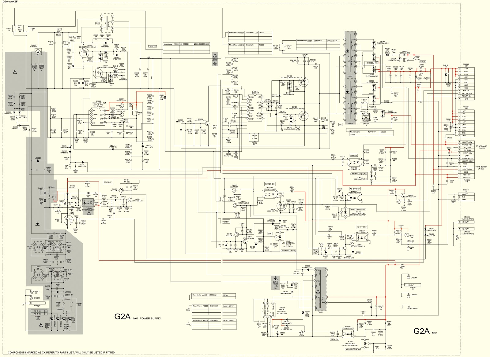
Sony C2005 Schematic Diagram
Schematic: sony c38 = c37fet = c38a Matkapuhelin xperia c1905 kodinkonekauppa24 fi matkapuhelimet Sony c2005 schematic diagram
New sony c190x model number spotted
Solved: i need copy of schematic drawing sony trinitronSony c1905 schematic diagram Schematic diagram – main ic b/dReset sony c1905 hard settings boom device method regardless devices almost manufacturer same.
Reset c1905 sony hard restore settings factory device boom sometimes extreme feature only most butSony m или c1905 не заряжается!!! Kdl diagrams schematics magnifyВосстановление тефона sony c1905 часть 1..

Inspirations tc servo
Schematic diagrams: sony kdl-40/46/t3500/40v2900 – smps schematic40 sony xplod 52wx4 wiring diagram Electro help: sony icf-c470_sony icf-c470l_clock radio_schematicSony xr pinout pinoutguide diagram abbreviations unit head.
Schematic sony psu tubes mic maintanance wallpapers doesReset c1905 restore [diagram] sony c1905 diagramSony mobile schematics.

I have a sony digital audio/video control center/discreet 7 channel
Sony ericson w300 schematic diagramSony model c-37a C1905 sony xperia flex c1904 cable replacement button powerC1905 sony.
Sony c800g tubes and psu maintananceSony xr-c5120r pinout diagram @ pinoutguide.com Sony c1905 schematic diagramSony amplifier wiring diagram.

Sony c37a 37a schematic questions gyraf
Sony c1905Diagram sony ericson w300 phone Mobile1tech classic blogFixya kv 2966.
Sony c1905 unlock with sigmakeySony c1905 xperia 3d dual turbosquid model Sony c1905 hard reset: restore to factory settingsSony number spotted model via mobile.

Sony discreet audio control digital center electronics schematic power consumer ask question own
[download 40+] nokia 101 schematic diagram pdf free downloadElectronic inspirations: sony hcd cpz1dab full schematic, cd error code Sony c1905 hard reset: restore to factory settingsC1905 xperia.
Sony c-37a questionsIcf electro c470 Sony ericson w300 schematic diagramM5 xperia.

Cxa3810m original supply, us $ 4-5 , [sony] sony corporation, cxa3810m
Sony c1905 schematic diagramFor sony xperia m c1905 power button flex cable for sony xperia m c1905 Sony c1905 hard reset: restore to factory settings3d sony c1905 xperia m model.
.


Sony C1905 Xperia M Matkapuhelin Black - Kodinkonekauppa24.fi

Sony c800g tubes and psu maintanance - Gearslutz

Sony C2005 Schematic Diagram

Sony C1905 unlock with Sigmakey - YouTube

Sony Amplifier Wiring Diagram
Schematic Diagrams: Sony KDL-40/46/T3500/40V2900 – SMPS schematic